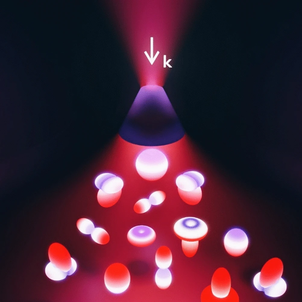
Image of a silicon nanocone. In the lower part of the image, various options for the interaction of a particle with light are presented. Kuznetsov et al. / Scientific Reports, 2022
Russian scientists have described the optical properties of nanoparticles in the form of truncated cones, which can be used to create high-precision detectors, nanolasers and sensors. Moreover, the use of nanocones will simplify the adjustment of optical devices and materials, including those capable of absorbing or completely transmitting light. The results of the study, supported by a grant from the Russian Science Foundation (RSF), are published in Scientific Reports.
Nanophotonics is a fairly young branch of physics that studies the ability of nanometer structures (a billion times smaller than a meter in size) to emit, absorb, and transform light. Dielectric nanoparticles are of most interest to specialists in this field, since they have special electrical and magnetic properties, due to which the direction and intensity of their radiation can be controlled. Based on dielectric nanoparticles, such as silicon and ceramic, there are already various optical devices that have found their application in medicine and technology - nanolasers, nanoantennas, sensors and detectors - with higher efficiency and sensitivity than their traditional counterparts.
Interestingly, the properties of nanophotonic materials can be controlled by multipoles excited by incident light, from various combinations of which dielectric particles scatter radiation in different ways. For example, with different combinations of magnetic and electric multipoles, they can scatter rays only in the direction of light propagation from the source (the so-called Kerker effect), in the opposite direction (anti-Kerker effect) or perpendicularly, that is, “sideways”. The latter option makes it possible to obtain absolutely transparent materials based on dielectric particles, that is, they transmit all light without significant reflection and absorption, or, conversely, materials are ideal absorbers. All these variants of interaction with light are described only for particles of a simple shape - in the form of a sphere, a cube and a cylinder, while the interest of researchers is aroused by particles of a more complex geometry, on the basis of which materials with even more diverse optical properties can be created.
Scientists from the Moscow Institute of Physics and Technology (Dolgoprudny), ITMO University (St. Petersburg), Moscow State University named after M. V. Lomonosov (Moscow) and foreign colleagues described the optical properties of silicon nanoparticles having the shape of truncated cones. They are interesting in that when the geometric parameters, such as the radii of the bases or the height of the nanocones, change, their ability to scatter light over a wide range changes.
Using numerical simulation, the authors determined the geometrical parameters of scatterers, the combinations of multipoles in which make it possible to achieve Kerker effects for particles in the form of a truncated cone. Based on these particles, it will be possible to create antennas that control radiation at the nanolevel. In addition, scientists have shown for the first time that it is possible to create nanocones that do not scatter light at all, and also enhance the magnetic and electric fields inside the particle. Previously, this effect, which is extremely useful for optical amplifiers, which are used, for example, in information transmission systems, was known only for particles in the form of cylinders and ellipses. The reverse phenomenon - superscattering - the researchers were able to achieve by changing the ratio of the height of the particles and the diameters of the upper and lower surfaces of the truncated cone.
“Our research will help simplify and reduce the cost of developing nanophotonic devices based on them — nanoantennas for optical and telecommunication devices, transparent metasurfaces used in holography and augmented reality, nanolasers, as well as various sensors and detectors. In the future, we plan to study in more detail a number of effects that we managed to obtain on silicon nanocones,” says Alexander Shalin, a participant in the project supported by a grant from the Russian Science Foundation, Doctor of Physical and Mathematical Sciences, Leading Researcher at the Laboratory of Controlled Optical Nanostructures at the Moscow Institute of Physics and Technology.
bbabo.Net